Nano Photonics
Slot Waveguide Coupling
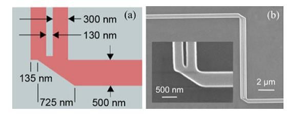
In recent years, great efforts have been dedicated to increase the compatibility of silicon photonics with the standard CMOS fabrication process. In order to have electronic and photonic devices coexisting on the same chip, one challenge is the ability to utilize sharp bends for photonic devices as it is for electronics. However, photonic devices that are based on total internal reflection guiding approaches have mainly adiabatic structures for bends to avoid radiation losses.

Schematic and SEM experimental sample of the proposed slot waveguide with sharp bend.
By achieving momentum matching of the waveguides through an orthogonal junction placement, and maximizing modal overlap through an angled facet, coupling efficiency of ∼70% and 3-dB bandwidth of over 500 nm can be achieved. Through momentum matching via orthogonal waveguide placement, coupling characteristics comparable to that of direct butt coupler is attained.
Simulation and experimental fabrication is both conducted in this design. The orthogonal bend configuration presented can lead to more densely integrated silicon photonic circuits containing devices and interconnects that utilize both the Si wire and slot waveguides
Ultra-long Range Plasmonic Waveguide
Asymmetric Waveguide (ASHP) Structure for Ultra-long Range Plasmonic Waveguide.
The tradeoff over mode confinement and propagation loss is a critical issue in plasmonic waveguide structure. To reach highest figure of merit (FOM) , hybrid plasmonic waveguide (HPW) is proposed as one of the most promising design that could maintain both nanoscale footprint and micron scale propagation. Physically HPW could be regarded as mixed of surface plasmon polariton (SPP) mode and total internal reflection (TIR) mode.

(Left) Asymmetric waveguide architecture could be analyzed by two coupled plasmonic waveguides. (Right) The ultralow loss propagation could be supported by field symmetry engineering.
By field symmetric engineering, HPW could support ultra-long range propagating distance over several hundreds of microns. However, the symmetric condition also requires high degree of symmetric waveguide geometry, which makes fabrication highly difficult. For asymmetric waveguide architecture, field symmetry is still achievable by treating the whole waveguide as a coupled system. In this sense, structural or even mode symmetry is no needed.
The physics origin could be investigated from simplified 1-D structure. Transfer matrix method and coupled mode theory are employed to find the lowest loss associated with ASHP, which corresponds to field symmetry by the metal. For 2-D real design, the loss could be as small as 0.025dB/μm with mode area of 0.23μm^2.
Coupled Hybrid Plasmonics
Dynamically reconfigurable of nanoscale modulator utilizing coupled hybrid plasmonics
The balance between extinction ratio (ER) and insertion loss (IL) dictates strict trade-off when
designing travelling-wave electro-optic modulators. By field symmetry engineering, the loss could be maximized by strong field enhancement overlapped with lossy material with its epsilon near zero property. Exemplified by ITO with 1nm accumulation layer, the design features high extinction ratio as well as low insertion loss with extraordinary high figure of merit.

Coupled hybrid plasmonics modulator.
The field symmetry condition could be accomplished by coupled waveguide theory even without symmetry arrangement of waveguide structure. It provides us with great experimental flexibility for designing ultracompact modulator with any emerging active material.
The underlying design also could be utilized as electro-optic modulator or in any other optical applications to increase light matter interaction. It is noted that the real part of effective index possess strong modulation by electric biasing as well, which is suitable for designing Mach-Zhender type or split ring resonators switching.